


Hitachi Chemical Co Ltd announces the relocation of its Open Laboratory to Kawasaki City , Kanagawa Prefecture, in order to strengthen the laboratory’s functions.
The Open Laboratory was established to promote open innovation for semiconductor packaging materials and processes in cooperation with customers and, equipment and material manufactures. The new “Packaging Solution Center (tentative),” introducing cutting-edge semiconductor packaging equipment and almost three times larger than the current laboratory, will begin full operation in August 2018.
In advance of other chemical manufacturers, Hitachi Chemical founded the “JISSO Center,” the predecessor of the Open Laboratory, in 1994 to promote the development of packaging materials based on its own evaluation and analysis while offering its customers timely solutions. In 2014, the center renewed its operation as the “Open Laboratory” after expanding the packaging and evaluation equipment capabilities to deal with wafers 300 millimeters in diameter. In this way, Hitachi Chemical has developed optimal packaging materials and processes in pursuit of the early launch of advanced packages through co-creation with its customers, and equipment and material manufacturers.
The Open Laboratory, having welcomed customers from over 400 companies by the end of December 2016, has also achieved other notable outcomes, such as the one-third shorter development period of the die-attach film used for packaging memory chips.
Meanwhile, expectations for semiconductor packaging technologies are higher than ever, with the development of thinner chips and finer wires as well as widespread adoption of advanced packages, including fan-out packages, expected to boost the market. Since introducing the latest equipment is essential for continuing research and development of optimal materials and processes, Hitachi Chemical has decided to relocate the Open Laboratory to the more accessible location of Shin-Kawasaki, while at the same time expanding its scale and upgrading its functions.
The Packaging Solution Center will consist of a cleanroom and laboratory space equipped with state-of-the-art packaging equipment to accelerate next-generation package research and development, in addition to a consortium area to evaluate future packaging technologies in collaboration with customers and, equipment and and material manufactures, Boasting a total area of 4,900 square meters, roughly three times larger than the current laboratory, the new facility will triple the cleanroom floor space from the current 400 to slightly over 1,200 square meters and introduce highly advanced equipment capable of handling various types and sizes, ranging from 300 mm diameter wafers to 600 mm rectangle panels.
This upgrade will allow Hitachi Chemical to perform integrated assembly operations all in one place, from the advanced wafer process method of laser dicing*1 to forming fine patterns with steppers*2 at the panel level and even developing and evaluating 2.5D,*3 3D,*4 FOWLP,*5 and FOPLP*6 packages. Strengthening the facility’s functions will also help Hitachi Chemical advance its total solution services, for example, providing an optimal combination of packaging materials in multiple processes and offering application methods according to process conditions.
In addition, as the new site in Shin-Kawasaki is located about 20 minutes by train from Tokyo Station or a 30-minute drive from Haneda Airport, superior accessibility from within Japan and abroad is likely to encourage more active co-creation. Moreover, the Packaging Solution Center is also expected to further enhance open innovation by collaborating with the many semiconductor industry related companies and universities concentrated in the Shin-Kawasaki district, as well as by taking advantage of its consortium space equipped with the latest cutting-edge equipment and other resources.
Hitachi Chemical will step up its efforts to improve a wide range of materials technology capabilities as its forte and continue to create new products and businesses in the high-end field. Among the key policy measures in the 2018 Medium-Term Management Plan, Hitachi Chemical will focus on cluster business development to win the global competition by grouping different but related businesses and sharing strategies. The Packaging Solution Center will serve as a strategic base for the packaging material cluster business, where Hitachi Chemical will not solely supply materials and develop processes but play a leading role as a comprehensive solution provider, contributing to the realization of new highly advanced packages through open innovation with its customers, equipment manufacturers and materials makers.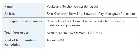 *1Dicing is the process in which a semiconductor wafer containing integrated circuits is diced into chips with a dicing saw (a high-precision cutting device using an industrial diamond rotary blade to cut workpieces, such as silicon glass and ceramics).
*2A stepper is an exposure device that projects a circuit pattern through the projector lens while moving around to print a circuit on a silicon or other semiconductor wafer.
*3A 2.5D package is a technology that produces IC chips arranged in parallel on a silicon interposer.
*4A 3D package is a technology that stacks chips using through-silicon via (TSV).
*5FOWLP (Fan-Out Wafer Level Package) is a type of wafer-level packaging that produces redistribution layers connecting between semiconductor chips and printed wiring substrates using the semiconductor manufacturing process. This package has a larger area than a semiconductor chip and can extend the terminal outside the chip.
*6FOPLP (Fan-Out Panel Level Package) is packaging implemented at the panel level rather than the wafer level for the above-mentioned FOWLP. Using a panel larger than a wafer allows many chips to be packaged at a time, improving productivity and lowering packaging costs.


